2026 Best Tips for Reverse Engineering PCB Techniques?
Reverse Engineering Pcb is a crucial skill in electronics. It involves analyzing and recreating printed circuit boards to understand their design and functionality. This process requires a blend of technical knowledge and practical experience. Engaging with reverse engineering opens doors to innovation and improvement, helping engineers learn from existing designs.
The techniques for reverse engineering PCB can vary widely. Successful engineers must familiarize themselves with tools and methodologies. Understanding the electronic components, layout, and manufacturing processes can reveal insights into product development. Yet, it's important to reflect on the ethical considerations in the industry. Challenges arise when balancing innovation and intellectual property rights.
As you explore the best tips for reverse engineering PCB technologies, consider your own experiences. Improvement comes from learning not only from successes but also from missteps. A critical approach to each project enhances understanding and fosters growth in this dynamic field. Embrace the journey to enrich your skills and elevate your expertise.
Understanding PCB Reverse Engineering: Key Concepts and Definitions
Reverse engineering printed circuit boards (PCBs) is a nuanced process that requires a deep understanding of key concepts. At its core, PCB reverse engineering involves analyzing a board to understand its structure and functionality. According to a 2022 report by IPC, the global PCB market is expected to reach $82 billion by 2025, driven largely by advances in electronic systems. This growth emphasizes the importance of reverse engineering as companies seek competitive advantages by deciphering innovative designs.
One of the critical aspects of PCB reverse engineering is the identification of components and materials used. Experts often focus on recognizing the types of components incorporated. For example, surface mount devices (SMDs) dominate modern designs, making familiarity with them essential. Research shows that nearly 70% of new designs utilize SMDs extensively. Additionally, understanding the manufacturing processes can uncover insights into design choices, helping engineers replicate or improve existing products.
Flaws are inherent in reverse engineering practices. Sourcing accurate data can sometimes be challenging. Misinterpretations may lead to incorrect conclusions about a PCB’s functionality. Autumn 2023 surveys indicate that about 30% of engineers reported issues related to unclear specifications. This underlines the importance of establishing well-defined parameters at the outset. Acknowledging these challenges is crucial for effective reverse engineering processes.
Essential Tools for Effective Reverse Engineering of PCBs
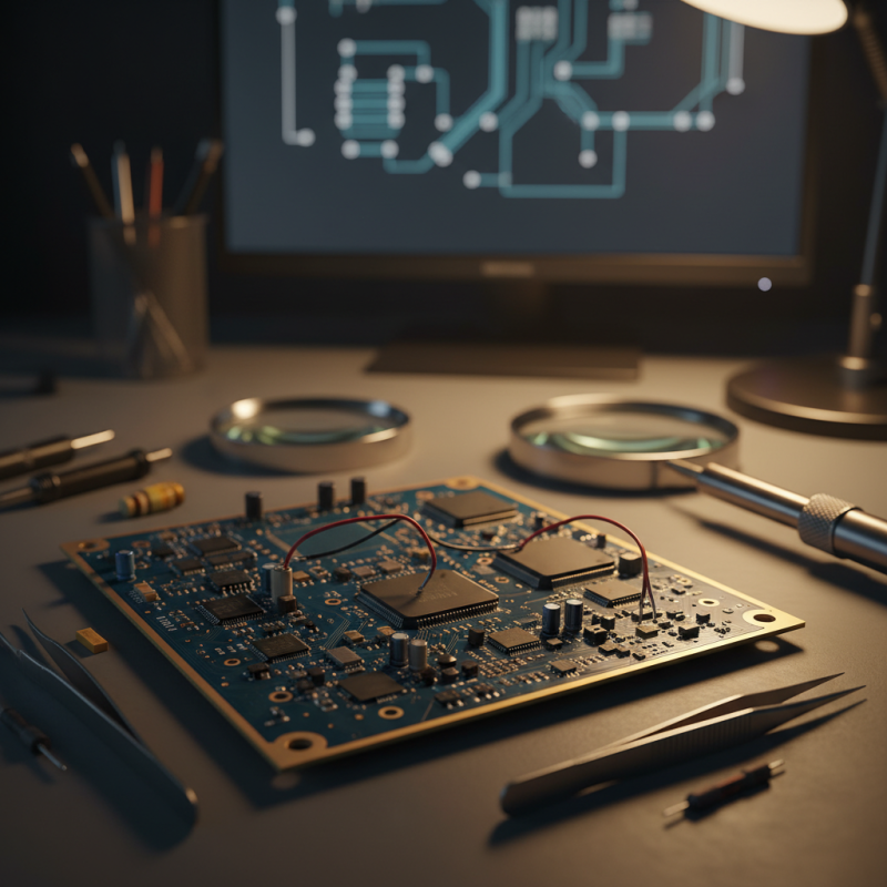
When embarking on reverse engineering PCBs, having the right tools is crucial. Start with a high-resolution microscope. This device allows you to examine the intricate details of the PCB. Observing the solder joints and trace routes becomes easier. A digital multimeter should also be part of your toolkit. It helps in measuring voltages and ohm resistance accurately. Both tools ensure precise data gathering, essential for successful analysis.
Next, consider using a thermal camera. It can detect hotspots on the PCB, indicating active components. This identification is key to understanding how each part functions within the circuit. Software for schematic capture and PCB design is also important. It allows you to recreate schematics based on your findings. Accuracy in this phase is vital, yet it can be a challenging process. You might encounter missing connections or unclear placements.
Documentation plays a significant role. Create detailed records of your assumptions and discoveries. Note any contradictions in your analysis, as they can reveal blind spots in your understanding. While these tools and processes may not guarantee instant success, they are essential steps toward mastering PCB reverse engineering. Embrace the learning curve and continue to refine your techniques as you go.
2026 Best Tips for Reverse Engineering PCB Techniques
| Technique | Description | Essential Tools | Skill Level |
| Schematic Extraction | Extracting the circuit schematic from a PCB. | Multimeter, Schematic capture software | Intermediate |
| PCB Layout Analysis | Analyzing layout to understand component placement. | CAD software, High-resolution scanner | Advanced |
| Component Identification | Identifying components used in the PCB. | Component database, Datasheets | Beginner |
| Reverse Engineering Software | Using software tools to analyze PCB designs. | Reverse engineering CAD tools | Expert |
| Signal Integrity Analysis | Assessing signal integrity of circuits. | Oscilloscope, Signal analysis software | Advanced |
Step-by-Step Process of Disassembling a PCB for Analysis
Disassembling a printed circuit board (PCB) requires careful attention and methodical steps. Start by gathering essential tools: a soldering iron, a multimeter, and a magnifying glass. Use the soldering iron to remove components. Heat the solder joints, then gently lift the parts with tweezers. This step can be tricky; overheating can damage the board.
Next, analyze the layout. Take photographs of the PCB for reference. Document the position of each component. Label them to avoid confusion later. Check for hidden connections. Sometimes traces are not obvious, and they can lead you to critical points. A magnifying glass can reveal fine details that might be missed by the naked eye.
It's crucial to reflect on the process. Every disassembly reveals something new; even mistakes can be educational. Maybe a wrong soldering technique caused a part to break. Learn from this. Continuously updating your methods based on past experiences will enhance your skills over time. Keep a detailed log of your observations. This will build your repository of knowledge and improve your reverse engineering techniques significantly.
Best Practices for Documenting Findings in PCB Reverse Engineering
Reverse engineering PCBs is a delicate process that requires accurate documentation. Effective documentation is crucial for respecting intellectual property while facilitating design improvements. A recent industry report indicates that 70% of engineers believe thorough documentation enhances project communication, leading to better outcomes.
Collecting data systematically involves clear labeling of components. This includes various resistors, capacitors, and ICs. Using standard nomenclature can help others understand your findings. A study by the IPC found that design teams spend an average of 30% of their time due to poor documentation practices. This emphasizes the need for clear visual aids and detailed notes.
Keeping track of measurements and configurations is another critical aspect. Photos and schematic diagrams should accompany written notes. Reflective practices, such as reviewing previous projects, can highlight common pitfalls in documentation. Continuous improvement is essential, as even small errors can lead to significant issues later on. Therefore, developing a reliable and consistent documentation strategy is paramount in reverse engineering PCB projects.
Common Challenges in PCB Reverse Engineering and How to Overcome Them
Reverse engineering printed circuit boards (PCBs) often presents unique challenges. Common regrets include poor documentation that complicates the reconstruction process. Many engineers find themselves stuck with outdated schematics, making the reverse engineering arduous. According to the IPC, improper documentation can lead to a 35% increase in design rework. It's vital to establish clear, concise notes during every stage of the reverse engineering cycle.
Another challenge is understanding complex component functionalities without manufacturer information. Many components may lack recognizable markings. This can lead to identification errors and additional reverse engineering time. A recent study by TechInsights highlighted that 60% of reverse engineering projects are delayed due to component identification issues. Utilizing advanced imaging technologies like X-ray microscopy can aid in revealing hidden layers and structures, improving the overall analysis.
Collaboration is also essential. Many engineers overlook the benefits of a multi-disciplinary approach. Engaging with experts from various fields can enhance problem-solving. When facing multifaceted PCB designs, integrating insights from electrical engineers, mechanical engineers, and even data analysts can streamline the process. This collaborative mindset can not only tackle immediate problems but foster innovation for future projects.